Core Digital Electronics: Flip-Flops, Logic Gates, Memory & ADCs
 English with a size of 514.7 KB
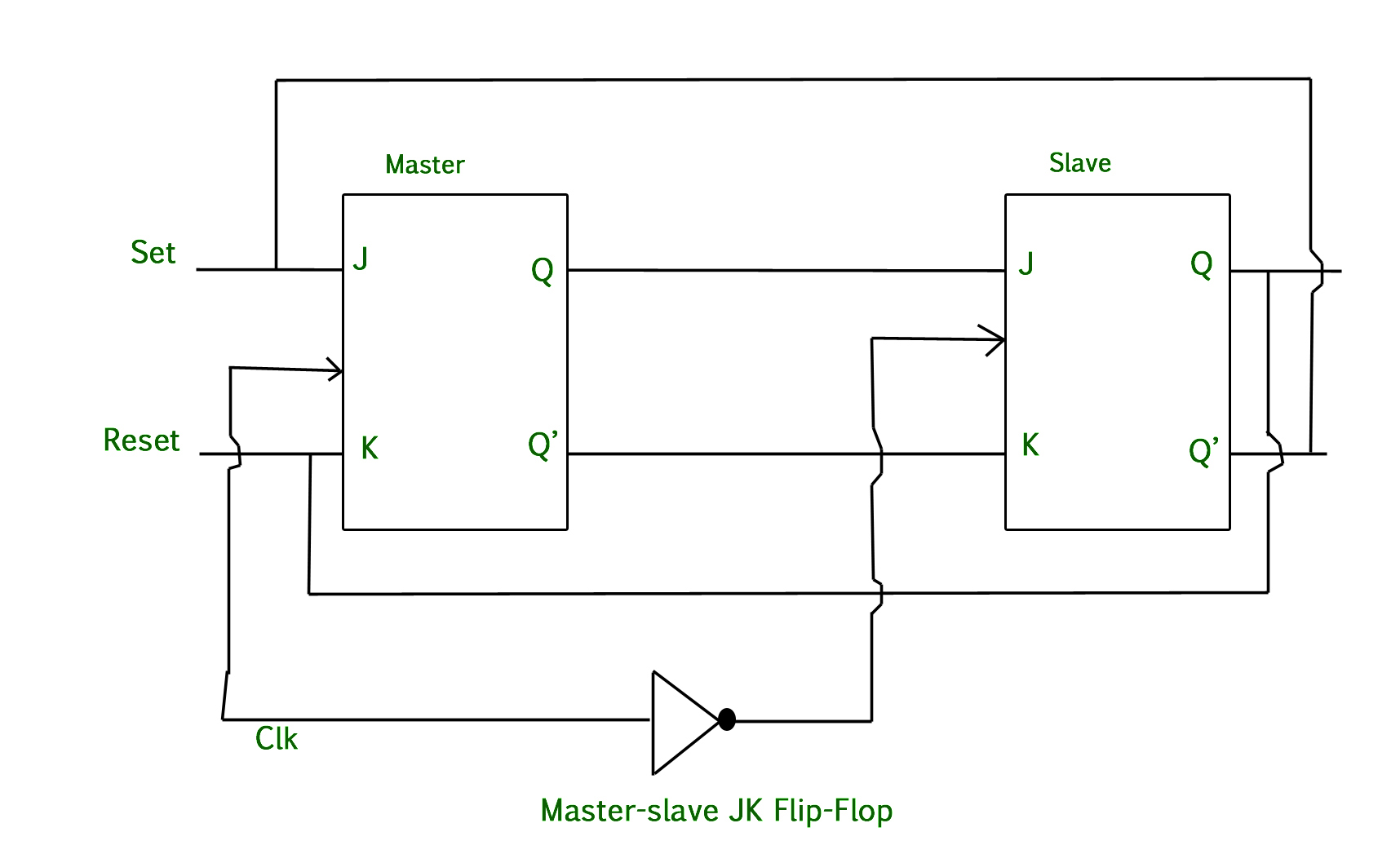
Master-Slave Flip-Flop Operation
The working of a Master-Slave flip-flop involves two cascaded flip-flops: a master and a slave. The master is positive level-triggered, and the slave is negative level-triggered, ensuring the master responds before the slave.
When the clock pulse (CP) goes high (1), the slave is isolated, allowing the J and K inputs to affect the master's state. The slave flip-flop remains isolated until the CP goes low (0). When the CP transitions back to low, information is passed from the master flip-flop to the slave, and the output is obtained.
Let's examine the behavior based on J and K inputs:
- J=0, K=1: The high Q' output of the master goes to the K input of the slave. The negative transition of the clock forces the slave to reset, thus the slave copies the master's reset state.
- J=1, K=0: The high Q output of the master goes to the J input of the slave. The negative transition of the clock sets the slave, copying the master's set state.
- J=1, K=1: The master toggles on the positive transition of the clock, and consequently, the slave toggles on the negative transition of the clock.
- J=0, K=0: The flip-flop is disabled, and the Q output remains unchanged.
Flash Analog-to-Digital Converter (ADC)
A Flash Analog-to-Digital Converter (ADC) is a type of ADC that utilizes a parallel architecture to convert an analog signal into a digital signal.
Operation of a Flash ADC
- Comparator Array: A bank of comparators compares the input analog signal to a set of precisely defined reference voltages.
- Reference Voltages: These reference voltages are accurately generated using a resistor ladder network.
- Digital Output: The outputs from all comparators are then fed into a digital encoder, which processes them to generate the final digital output.
Advantages of Flash ADCs
- High Speed: Flash ADCs are renowned as the fastest type of ADC, offering conversion times typically in the nanosecond range.
- Simple Architecture: Despite their speed, the fundamental architecture is relatively straightforward.
Limitations of Flash ADCs
- Limited Resolution: Flash ADCs are generally limited to around 8-bit resolution. This is due to the exponential increase in the number of comparators required (2n - 1 for n bits), making higher resolutions impractical.
- High Power Consumption: The large number of comparators operating simultaneously leads to significant power consumption.
Applications of Flash ADCs
- High-Speed Data Acquisition: Ideal for systems requiring rapid data capture.
- Real-Time Signal Processing: Used in applications where immediate processing of signals is crucial.
Flash ADCs are particularly suitable for applications where high speed is critical, and moderate resolution requirements are acceptable.
Understanding Priority Encoders
A priority encoder is a digital circuit designed to convert multiple input signals into a binary output signal, with the unique characteristic of prioritizing the highest-priority active input.
Key Features of Priority Encoders
- Multiple Inputs: Priority encoders are equipped with several input lines.
- Prioritization: Each input is assigned a specific priority level, ensuring that higher-priority active inputs take precedence over lower-priority ones.
- Binary Output: The circuit produces a binary code at its output, which uniquely represents the highest-priority input that is currently active.
Operation of a Priority Encoder
- Input Detection: The priority encoder first identifies which of its input lines are active (high).
- Priority Determination: It then evaluates all active inputs to determine which one holds the highest priority.
- Output Encoding: Finally, the encoder generates a corresponding binary output code for the highest-priority active input.
Applications of Priority Encoders
- Interrupt Handling: Widely used in computer systems and microcontrollers to prioritize multiple simultaneous interrupt requests.
- Digital Systems: Essential in various digital systems where multiple inputs must be managed and prioritized effectively.
Benefits of Using Priority Encoders
- Efficient Prioritization: They provide an efficient mechanism for handling and prioritizing multiple concurrent inputs.
- Simplified Design: By encapsulating complex prioritization logic, they significantly simplify the overall design of digital systems.
Priority encoders are fundamental components in digital systems, enabling robust and efficient prioritization and encoding of multiple inputs.
Essential Digital Circuit Components
Understanding various digital circuit components is fundamental to designing and implementing digital systems. Here, we detail ROM, RAM, PLA, and PAL.
ROM (Read-Only Memory)
- Definition: A type of non-volatile memory that stores permanent data.
- Characteristics: Data is typically written during manufacturing and cannot be easily modified or erased by the user.
- Applications: Commonly used for storing firmware (e.g., BIOS/UEFI), bootloaders, and other permanent data.
RAM (Random Access Memory)
- Definition: A type of volatile memory that stores temporary data.
- Characteristics: Data is lost when power is turned off. It allows for fast reading and writing of data.
- Applications: Serves as main memory in computers, cache memory, and for temporary data storage in various digital devices.
PLA (Programmable Logic Array)
- Definition: A type of programmable logic device (PLD) that can be programmed to implement complex logic functions.
- Characteristics: Both its AND plane and OR plane are programmable, offering high flexibility in implementing sum-of-products expressions.
- Applications: Used in digital logic implementation, control systems, and embedded systems where custom logic is required.
PAL (Programmable Array Logic)
- Definition: Another type of programmable logic device (PLD) designed to implement logic functions.
- Characteristics: In contrast to PLA, only the AND plane is programmable, while the OR plane is fixed. This simplifies design but offers less flexibility than PLAs.
- Applications: Widely used for digital logic implementation, control systems, and embedded systems, particularly when the logic functions are less complex than those requiring a PLA.
These components are crucial in the design and implementation of various digital systems, ranging from simple logic circuits to complex computing architectures.
Transistor-Transistor Logic (TTL) Explained
TTL (Transistor-Transistor Logic) is a prominent digital logic family that employs bipolar junction transistors (BJTs) to construct logic gates.
Key Characteristics of TTL
- Bipolar Transistors: TTL logic fundamentally uses BJTs for amplifying and switching digital signals.
- Standard Power Supply: TTL circuits typically operate with a 5V power supply.
- High Speed: TTL logic is known for its relatively fast operation, with propagation delays often in the nanosecond range.
TTL Logic Families
- Standard TTL: This is the original TTL family, offering a moderate balance of speed and power consumption.
- Low-Power TTL (LPTTL): A variant designed for lower power consumption, achieved by reducing current.
- Schottky TTL: A faster version of TTL that incorporates Schottky diodes to significantly improve switching speed and prevent transistor saturation.
Advantages of TTL
- High Speed: Its inherent speed makes TTL logic suitable for many high-speed digital applications.
- Wide Availability: TTL logic integrated circuits (ICs) are widely available, well-established, and have a long history of use.
Disadvantages of TTL
- Power Consumption: Compared to more modern logic families like CMOS, TTL logic consumes relatively high power.
- Limited Noise Immunity: TTL logic generally has more limited noise immunity compared to other logic families.
Applications of TTL
- Digital Electronics: TTL logic is extensively used in various digital electronic applications, including computers, communication systems, and control systems.
- Prototyping: Due to its simplicity and availability, TTL logic ICs are frequently used in the prototyping and development phases of digital systems.
Synchronous vs. Asynchronous Digital Circuits
Digital circuits can be broadly categorized into synchronous and asynchronous types, primarily distinguished by their timing mechanisms.
Synchronous Circuits
- Clock Signal: These circuits utilize a central clock signal to synchronize all internal operations.
- Clock-Driven: All state changes and data transfers occur precisely on a specific edge (rising or falling) of the clock signal.
- Predictable Behavior: Due to the synchronized clock, their behavior is highly predictable and deterministic, making them easier to design and debug.
Asynchronous Circuits
- No Clock Signal: Asynchronous circuits do not rely on a global clock signal for synchronization.
- Event-Driven: State changes are triggered directly by changes in input signals or internal events, rather than by a clock edge.
- Potentially Unpredictable Behavior: The absence of a clock can lead to variable timing and make their behavior harder to analyze and predict, especially in complex systems.
Key Differences
- Clocking Mechanism: Synchronous circuits are clock-dependent, while asynchronous circuits are clock-independent.
- Timing Characteristics: Synchronous circuits exhibit predictable and fixed timing, whereas asynchronous circuits have variable timing.
- Design Complexity: Synchronous circuits are generally considered easier to design, analyze, and verify. Asynchronous circuits, while potentially faster and lower power, can be significantly more complex to design and ensure correct operation.
Understanding Ring Counters
A ring counter is a specialized type of digital counter composed of a series of flip-flops connected in a circular fashion, where the output of the last flip-flop feeds back into the input of the first.
Operation of a Ring Counter
- Initial State: Typically, one flip-flop is initially set to a logic '1', while all other flip-flops in the ring are reset to '0'.
- Clock Pulse: With each subsequent clock pulse, the logic '1' is shifted sequentially from one flip-flop to the next around the circular arrangement.
Characteristics
- Circular Shift: The '1' bit continuously shifts in a circular pattern, eventually returning to the first flip-flop after traversing the entire ring.
- Sequence Generation: Ring counters are inherently designed to generate a specific, repeating sequence of states.
Applications
- Frequency Division: They can be effectively used to divide input clock frequencies.
- Sequence Generation: Ideal for applications that require the generation of precise, repeating digital sequences.
Types of Ring Counters
- Simple Ring Counter: This is the basic configuration where a single '1' bit shifts through the flip-flops.
- Johnson Counter (Twisted Ring Counter): A variation of the ring counter that incorporates an inverted feedback from the last flip-flop to the first, generating a different sequence length.
Ring counters are valuable components in digital systems for their ability to generate sequences and perform frequency division.
Twisted Ring Counter (Johnson Counter)
A twisted ring counter, more commonly known as a Johnson counter, is a specialized type of digital counter. It comprises a series of flip-flops connected circularly, but with a crucial difference: the inverted output of the last flip-flop is fed back to the input of the first flip-flop.
Operation
- Initial State: Typically, all flip-flops are initially reset to '0'.
- Clock Pulse: With each clock pulse, the data shifts through the flip-flops. The inverted output (Q') of the last flip-flop is then fed back as the input to the first flip-flop.
Characteristics
- Sequence Generation: Johnson counters generate a unique and specific sequence of states.
- Sequence Length: For a counter with 'n' flip-flops, the sequence length is 2n, which is twice the length of a simple ring counter with the same number of flip-flops.
Applications
- Sequence Generation: Widely used in applications that require the generation of specific, repeating digital sequences.
- Digital Control Systems: Employed in various digital control systems for generating precise control signals.
Advantages
- Simple Design: Johnson counters generally have a relatively straightforward design.
- Flexibility: They can be adapted to generate a variety of different sequences, making them versatile.
Johnson counters are valuable in digital systems for their ability to generate specific sequences and effectively control digital circuits.
Encoder vs. Decoder: A Detailed Comparison
Encoders and decoders are fundamental digital logic circuits that perform inverse operations, crucial for data manipulation in various systems.
Encoder
- Function: An encoder converts data or a signal from one format into a coded form, typically using a specific algorithm or scheme.
- Input: It accepts an input signal or data, often with multiple input lines.
- Output: It produces a coded output signal or data, usually with fewer output lines than input lines.
- Purpose: Encoders are primarily used for data compression, encryption, or converting a decimal or octal input into a binary code.
Decoder
- Function: A decoder performs the inverse operation of an encoder; it converts a coded signal or data back into its original, uncoded form using a specific algorithm or scheme.
- Input: It takes in a coded input signal or data.
- Output: It produces the original, uncoded output signal or data, often with more output lines than input lines.
- Purpose: Decoders are used for data decompression, decryption, or converting a binary code into a decimal or octal output, or for activating specific output lines based on an input code.
Key Differences
- Direction of Conversion: Encoders convert data into a coded form, while decoders convert coded data back into its original form.
- Functionality: They have opposite functions; encoders map multiple inputs to a unique code, and decoders map a code to a unique output.
Common Applications
- Data Transmission: Both are used in data transmission systems to ensure efficient and secure data transfer (e.g., encoding before transmission, decoding upon reception).
- Data Storage: Employed in data storage systems for compressing or encrypting data to save space or enhance security.
Examples
- Text Encoding: ASCII encoding is a classic example of encoding text characters into binary codes. Decoding would involve converting these ASCII codes back into readable text.
- Audio/Video Encoding: Audio/video codecs (e.g., MP3, H.264) extensively use encoding to compress multimedia data for storage and transmission, and decoding to decompress it for playback.
J-K Flip-Flop Race-Around Condition & Solutions
Understanding the Race-Around Condition
The race-around condition is a critical issue that can occur in a J-K flip-flop when both J and K inputs are simultaneously high (logic 1) and the clock pulse (CP) remains high for an extended duration. This scenario causes the flip-flop's output to toggle repeatedly and uncontrollably during the active clock pulse period, leading to unpredictable and unreliable behavior.
Causes of Race-Around
- Feedback Loop: The inherent feedback mechanism within the J-K flip-flop design can lead to oscillation of the output when both J and K inputs are high.
- Excessive Clock Pulse Width: If the clock pulse width is too long, it allows sufficient time for the output to toggle multiple times before the clock pulse ends.
Measures to Rectify
To effectively mitigate or eliminate the race-around condition, several design strategies can be employed:
- Master-Slave J-K Flip-Flop: Implementing a master-slave configuration is a common solution. This design ensures that the output changes only once per complete clock cycle, effectively isolating the inputs from the outputs during the active clock phase.
- Edge-Triggered Flip-Flops: Utilizing edge-triggered flip-flops, which respond only to the rising or falling edge of the clock pulse (rather than the entire level), inherently prevents the race-around condition by limiting the time window for state changes.
- Clock Pulse Width Control: Ensuring that the clock pulse width is carefully controlled and made shorter than the propagation delay of the flip-flop can also help prevent multiple toggles within a single clock cycle.
By implementing these measures, the race-around condition can be effectively mitigated, ensuring reliable and predictable operation of J-K flip-flops in digital circuits.
Deriving J-K Flip-Flop Complement Output Equation
To demonstrate that the characteristic equation for the complement output (Q') of a J-K flip-flop is Q'(t+1) = J'Q' + KQ, we begin with the known characteristic equation for the Q output.
Starting with Q(t+1)
The characteristic equation for the Q output of a J-K flip-flop is:
Q(t+1) = JQ' + K'Q
Complement Output Q'(t+1)
The complement output Q'(t+1) is, by definition, the inverse of Q(t+1):
Q'(t+1) = (Q(t+1))'
Substituting the equation for Q(t+1):
Q'(t+1) = (JQ' + K'Q)'
Applying De Morgan's Law
Using De Morgan's Law (A+B)' = A'B', we can expand the expression:
Q'(t+1) = (JQ')' * (K'Q)'
Applying De Morgan's Law again ((AB)' = A' + B') to each term:
Q'(t+1) = (J' + Q) * (K + Q')
Simplification to Final Form
Expanding the product yields J'K + J'Q' + QK + QQ'. Since QQ' = 0 (complement law), this simplifies to J'K + J'Q' + QK.
While algebraic simplification from this point can be complex, using a Karnaugh map (K-map) for Q'(t+1) based on the J-K flip-flop's truth table directly yields the simplified form:
Q'(t+1) = J'Q' + KQ
This confirms that the characteristic equation for the complement output Q' of a J-K flip-flop is indeed Q'(t+1) = J'Q' + KQ.

Converting D Flip-Flops to J-K and S-R
A D flip-flop is primarily designed to provide a delay, as its output directly mirrors its input after a clock pulse. While D flip-flops can be constructed from S-R or J-K flip-flops, designers often need to convert a D flip-flop into other types, such as J-K or S-R flip-flops.
The conversion process typically involves two main steps:
- Truth Table Creation: First, draw the excitation tables or truth tables for both the target flip-flop (e.g., J-K or S-R) and the available flip-flop (the D flip-flop).
- Karnaugh Map (K-Map) Derivation: Next, create the equivalent Karnaugh Maps (K-Maps) for the required inputs of the D flip-flop, based on the desired behavior of the target flip-flop. This helps in deriving the logic gates needed for the conversion.


10-bit Binary-Ladder DAC Calculations
For a 10-bit Binary-Ladder type Digital-to-Analog Converter (DAC) with a reference voltage (Vref) of 10V, let's determine key performance parameters.
(a) Output Voltages Caused by Each Bit
The output voltage contributed by each bit (Vn) in a binary-ladder DAC can be calculated using the formula:
Vn = Vref * (2(n-1) / 210)
where 'n' represents the bit position (from 1 for LSB to 10 for MSB).
Calculating output voltages for each bit:
- Bit 10 (MSB): V10 = 10V * (29 / 210) = 5V
- Bit 9: V9 = 10V * (28 / 210) = 2.5V
- Bit 8: V8 = 10V * (27 / 210) = 1.25V
- Bit 7: V7 = 10V * (26 / 210) = 0.625V
- Bit 6: V6 = 10V * (25 / 210) = 0.3125V
- Bit 5: V5 = 10V * (24 / 210) = 0.15625V
- Bit 4: V4 = 10V * (23 / 210) = 0.078125V
- Bit 3: V3 = 10V * (22 / 210) = 0.0390625V
- Bit 2: V2 = 10V * (21 / 210) = 0.01953125V
- Bit 1 (LSB): V1 = 10V * (20 / 210) = 0.009765625V
(b) Output Voltage for Digital Input 1101010100
To calculate the total output voltage (Vout), we sum the individual bit voltages for each bit that is set to '1' in the digital input 1101010100 (from MSB to LSB):
Vout = V10 + V9 + V7 + V5 + V3
Vout = 5V + 2.5V + 0.625V + 0.15625V + 0.0390625V
Vout = 8.3203125V
(c) Full Scale Voltage (Vfs)
The full scale voltage (Vfs) represents the maximum possible output voltage the DAC can produce, which is slightly less than Vref:
Vfs = Vref * (1 - 1/210)
Vfs = 10V * (1 - 1/1024)
Vfs = 10V * (1023/1024)
Vfs = 9.990234375V
(d) DAC Resolution
The resolution of the DAC is the smallest possible change in the output voltage, corresponding to a change of one LSB:
Resolution = Vref / 210
Resolution = 10V / 1024
Resolution = 0.009765625V
This resolution value signifies the smallest increment in output voltage that can be achieved by this 10-bit DAC.
Edge-Triggered RS Flip-Flop Advantages
Edge-triggered RS flip-flops offer significant advantages over traditional clocked or gated (level-sensitive) RS flip-flops, primarily in terms of reliability and timing precision in digital circuits.
Key Advantages
- Improved Noise Immunity: Edge-triggered flip-flops are considerably less susceptible to noise and glitches present on the input signals. This is because they only sample and respond to the input signals at the precise moment of a clock edge (either rising or falling), ignoring input changes during the rest of the clock cycle.
- Reduced Metastability: They are less prone to metastability issues, which can arise when input signals are unstable or change simultaneously with the active clock level in level-sensitive designs. Edge-triggering provides a narrower window for input changes, reducing the likelihood of an indeterminate state.
- Better Timing Control: Edge-triggered flip-flops provide superior control over the timing of output signals. Output changes are strictly synchronized to the clock edge, leading to more predictable and precise system behavior.
Comparison to Level-Sensitive RS Flip-Flops
- Level-Sensitive (Clocked/Gated) RS Flip-Flops: These flip-flops are sensitive to the logic level of the clock signal. The output can change as long as the clock signal is active (e.g., high), making them vulnerable to input changes throughout that entire period.
- Edge-Sensitive (Edge-Triggered) RS Flip-Flops: In contrast, these flip-flops are sensitive only to the transition (edge) of the clock signal. The output changes exclusively at the rising or falling edge, providing a much tighter control window.
The enhanced performance and reliability of edge-triggered RS flip-flops make them a preferred choice in many modern digital circuit applications, especially where precise timing and noise robustness are critical.
RTL (Resistor-Transistor Logic) NOR Gate
The RTL (Resistor-Transistor Logic) NOR gate is a fundamental logic gate implemented using bipolar junction transistors and resistors. It performs the logical NOR operation.
Circuit Structure
An RTL NOR gate typically consists of two or more NPN bipolar junction transistors connected in parallel. Resistors are connected to the base of each transistor, and a common collector resistor is used for the output.
Operation
- Input Signals: Input signals (A, B, etc.) are applied to the base of each transistor through their respective base resistors.
- Transistor Switching: If any input signal is high (logic 1), the corresponding transistor turns on (saturates). This effectively creates a low-resistance path from the output to ground, pulling the output voltage low (logic 0).
- Output State: If all input signals are low (logic 0), all transistors remain off (in cutoff). In this state, the output voltage is pulled high (logic 1) through the collector resistor.
Truth Table
| A | B | Output |
|---|---|---|
| 0 | 0 | 1 |
| 0 | 1 | 0 |
| 1 | 0 | 0 |
| 1 | 1 | 0 |
Summary of Working
- All Inputs Low: When both inputs (A and B) are low (0), both transistors are off, and the output is high (1).
- Any Input High: When either input (A or B, or both) is high (1), the corresponding transistor(s) turn on, pulling the output low (0).
Thus, the RTL NOR gate correctly implements the logical NOR operation, producing a high output only when all its inputs are low.
Logic Family Comparison: RTL, DTL, TTL, CMOS
Understanding the characteristics of different logic families is crucial for selecting the appropriate technology for digital circuit design. Here's a comparative table of RTL, DTL, TTL, and CMOS based on key parameters:
| Logic Family | Fan-In | Fan-Out | Noise Margin | Power Dissipation | Propagation Delay |
|---|---|---|---|---|---|
| RTL (Resistor-Transistor Logic) | Limited | Low (5-10) | Low | Medium | Medium |
| DTL (Diode-Transistor Logic) | Limited | Medium (8-12) | Medium | Medium | Medium |
| TTL (Transistor-Transistor Logic) | Medium | High (10-20) | Medium | High | Low-Medium |
| CMOS (Complementary Metal-Oxide-Semiconductor) | High | High (50-100) | High | Low | Low-Medium |
Key Observations
- Fan-In: CMOS typically offers the highest fan-in capability, largely due to its high input impedance.
- Fan-Out: Both CMOS and TTL exhibit high fan-out capabilities, allowing them to drive a larger number of subsequent gates.
- Noise Margin: CMOS stands out with the highest noise margin, indicating superior immunity to electrical noise.
- Power Dissipation: CMOS is highly advantageous for low-power applications due to its significantly lower static power dissipation.
- Propagation Delay: TTL and CMOS generally provide relatively low propagation delays, making them suitable for high-speed operations.
This comparison effectively highlights the strengths and weaknesses of each logic family, assisting designers in choosing the most suitable technology for their specific application requirements.
ROM Types & PC Memory Architecture
Read-Only Memory (ROM) is a crucial component in digital systems, known for its non-volatile nature. Various types of ROM have evolved over time, each with distinct characteristics.
Types of Read-Only Memory (ROM)
- Mask ROM (MROM): Programmed during the manufacturing process. Data is permanently stored and cannot be modified by the user.
- Programmable ROM (PROM): Can be programmed once by the user (using a PROM programmer). Once programmed, the data is permanent and non-modifiable.
- Erasable Programmable ROM (EPROM): Programmable by the user and can be erased using intense ultraviolet (UV) light, allowing for re-programming.
- Electrically Erasable Programmable ROM (EEPROM): Programmable, erasable, and re-programmable electrically, offering more flexibility than EPROM.
- Flash Memory: A modern type of non-volatile memory that can be electrically erased and re-programmed in blocks, making it highly versatile.
ROM Usage in Modern PCs
Modern Personal Computers (PCs) predominantly utilize Flash Memory. Specifically, the UEFI (Unified Extensible Firmware Interface) firmware, which replaces the traditional BIOS, is stored in a Flash ROM chip located on the motherboard.
Input and Output Lines in PC ROM
The exact number of input (address) and output (data) lines in a PC's ROM chip varies based on the specific chip model and system architecture. However, for a typical Flash ROM chip:
- Address Lines: Typically 16 to 24 lines, depending on the total memory size the chip can address.
- Data Lines: Usually 8 or 16 lines, determining the data width that can be read simultaneously.
Calculating Total ROM Memory
Assuming a common scenario for UEFI firmware, such as a 16 MB (128 Mb) Flash ROM chip with an 8-bit data width and a 24-bit address space:
- Address Lines: 24 (allowing 224 unique memory locations)
- Data Lines: 8 (meaning 8 bits or 1 byte per memory location)
- Total Memory: 224 bytes = 16,777,216 bytes = 16 MB (or 128 Megabits).
It's important to note that the actual memory size and organization can vary significantly depending on the specific PC model and the ROM chip employed.
Static RAM (SRAM) vs. Dynamic RAM (DRAM)
Static RAM (SRAM) and Dynamic RAM (DRAM) are two primary types of Random Access Memory, each with distinct characteristics that make them suitable for different applications.
Static RAM (SRAM)
- Memory Cell Structure: SRAM utilizes flip-flop circuits (typically 6 transistors) to store each bit of data.
- Refresh Requirement: SRAM retains data as long as power is supplied, meaning it does not require periodic refresh cycles.
- Access Speed: SRAM offers significantly faster access times compared to DRAM.
- Cost: Due to its complex cell structure, SRAM is generally more expensive per bit than DRAM.
Dynamic RAM (DRAM)
- Memory Cell Structure: DRAM stores each bit of data using a capacitor and a single transistor.
- Refresh Requirement: Capacitors naturally discharge over time, so DRAM requires periodic refresh cycles to maintain the stored data.
- Access Speed: DRAM has slower access times compared to SRAM because of the refresh cycles and the need to charge/discharge capacitors.
- Cost: With its simpler cell structure, DRAM is less expensive per bit, allowing for higher memory densities.
Key Differences Summarized
- Memory Cell: SRAM uses flip-flops; DRAM uses capacitors.
- Refresh: SRAM does not require refresh cycles; DRAM requires periodic refresh.
- Speed & Cost: SRAM is faster but more expensive; DRAM is slower but less expensive.
SRAM is typically chosen for applications demanding very fast access times and low latency, such as CPU cache memory. DRAM, on the other hand, is preferred for applications requiring large memory capacities at a lower cost, making it ideal for main system memory.
Calculating Bits for ADC Resolution
To determine the minimum number of bits required for an Analog-to-Digital Converter (ADC) to achieve a specific voltage resolution with a given full-scale voltage, we use the resolution formula.
Determining Number of Bits
The resolution of a converter is defined as:
Resolution = Full Scale Voltage / (2n - 1)
where 'n' is the number of bits.
Given Parameters
- Full Scale Voltage (FSV): 10V
- Desired Resolution: 5mV = 0.005V
Calculation Steps
Substitute the given values into the resolution formula:
0.005V = 10V / (2n - 1)
Rearrange the equation to solve for 2n - 1:
2n - 1 = 10V / 0.005V
2n - 1 = 2000
Add 1 to both sides:
2n = 2001
To find 'n', take the logarithm base 2 of 2001:
n = log2(2001)
n ≈ 10.97
Conclusion
Since the number of bits ('n') must be an integer, we must round up to the nearest whole number to meet or exceed the desired resolution.
Therefore, 11 bits are required at the input of the converter to resolve voltages to 5mV with a full-scale voltage of +10V.
Dual-Slope Analog-to-Digital Converter (ADC)
The Dual-Slope ADC is a type of Analog-to-Digital Converter known for its high accuracy and noise rejection capabilities, making it suitable for precision measurement applications.
Principle of Operation
The core principle of a dual-slope ADC involves converting an analog input signal into a digital output by performing two integration phases. First, the input signal is integrated for a fixed duration. Second, a known reference voltage of opposite polarity is integrated until the integrator's output returns to its starting point (zero).
Operational Phases
- Integration Phase: The unknown analog input voltage is applied to an integrator circuit and integrated for a precisely fixed time period. During this phase, the integrator's output voltage ramps up (or down) proportionally to the input voltage.
- De-integration Phase: After the fixed integration time, the input is switched off, and a stable reference voltage (of opposite polarity to the input) is applied to the integrator. This causes the integrator's output to ramp back towards zero.
- Conversion: A counter measures the time taken for the integrator's output to return to zero during the de-integration phase. This measured time is directly proportional to the amplitude of the original analog input signal, thus providing the digital equivalent.
Advantages
- High Accuracy: Dual-slope ADCs are renowned for offering excellent accuracy and linearity, as the conversion is less dependent on the absolute values of the integrating capacitor and resistor.
- Noise Rejection: They possess good inherent noise rejection capabilities, particularly for power line frequencies, due to the integration process.
Applications
- Precision Measurements: Widely used in digital multimeters, data loggers, and other instruments requiring high-precision measurements.
- Industrial Control: Employed in industrial control systems where accuracy and stability are paramount.
Characteristics
- Slow Conversion Rate: Compared to other ADC types like Flash ADCs, dual-slope ADCs have significantly slower conversion rates due to the two-phase integration process.
- High Resolution: They are capable of achieving very high resolutions.
Dual-slope ADCs are an excellent choice for applications where high accuracy and precision are critical, even if it means sacrificing some conversion speed.
Expected Accuracy of a 10-bit ADC
The overall accuracy of an Analog-to-Digital Converter (ADC) is a critical performance metric, often expressed in terms of its Least Significant Bit (LSB). Let's determine the reasonable accuracy for a 10-bit ADC.
Resolution Calculation
A 10-bit ADC is capable of distinguishing between 210 discrete levels. Therefore:
Number of Levels = 210 = 1024 levels
LSB Value for a 10V Full-Scale Range
Assuming a full-scale input range of 10V, the value of one LSB can be calculated as:
LSB = Full-Scale Range / Number of Levels
LSB = 10V / 1024 ≈ 0.009765625V ≈ 9.77mV
Overall Expected Accuracy
The overall accuracy of an ADC is typically specified as a fraction of the LSB, accounting for various errors (quantization, linearity, offset, gain). A reasonable expectation for a well-designed 10-bit ADC is an accuracy ranging from ±1/2 LSB to ±1 LSB.
- ±1/2 LSB Accuracy: ± (9.77mV / 2) = ±4.885mV
- ±1 LSB Accuracy: ±9.77mV
Therefore, one could reasonably expect the overall accuracy of a 10-bit ADC to be in the range of ±4.885mV to ±9.77mV, depending on the specific design, calibration, and quality of the ADC.